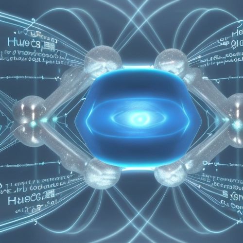
The emerging field of topological insulators has revolutionized our understanding of electronic conduction at material interfaces. Unlike conventional insulators, these exotic materials possess conducting surface states while maintaining an insulating bulk, creating unique opportunities for controlling electron flow at their boundaries. Recent breakthroughs in interface engineering have unlocked unprecedented control over these surface states, paving the way for novel quantum devices and energy-efficient electronics.
At the heart of topological insulator behavior lies the intricate dance between spin and momentum of surface electrons. The spin-momentum locking phenomenon creates helical states where electron spin orientation becomes intrinsically tied to its direction of motion. This property, protected by time-reversal symmetry, gives rise to robust conduction channels that are remarkably resistant to backscattering from non-magnetic impurities. Researchers have discovered that carefully engineered interfaces can manipulate these protected states without destroying their topological character.
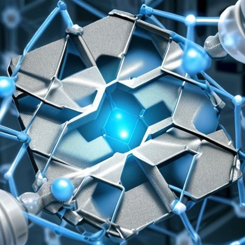
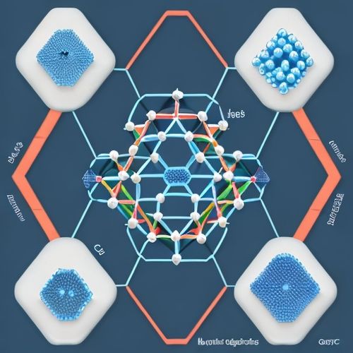
Interface engineering has emerged as the most promising approach to harness topological surface states for practical applications. By creating heterostructures with conventional semiconductors or superconductors, scientists can tune the Dirac point position and modify the surface state dispersion. The key breakthrough came with the realization that interface potential gradients could spatially confine topological states while preserving their unique transport properties. This confinement enables the creation of topological nanowires and quantum dots with tailored electronic characteristics.
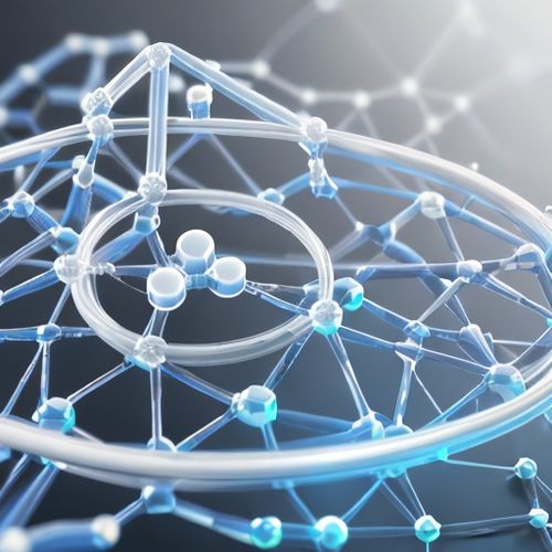
The marriage between topological insulators and superconducting materials has produced particularly fascinating results. When brought into proximity with superconductors, the topological surface states can inherit superconducting correlations through the proximity effect. This combination creates a playground for Majorana fermions - exotic particles that are their own antiparticles. The interface between these materials requires atomic-level precision, as even minor defects can disrupt the delicate balance needed to observe these quantum phenomena.
Magnetic doping presents another powerful knob for controlling interface conduction in topological insulators. Introducing magnetic atoms at the interface breaks time-reversal symmetry, opening a gap in the surface state spectrum. This magnetic tuning allows researchers to switch between conductive and insulating surface states, creating possibilities for topological transistors. The challenge lies in achieving uniform doping without introducing excessive disorder that could mask the topological effects.
Recent experiments have demonstrated that interface chemistry plays a crucial role in determining conduction properties. Oxidation states, interfacial charge transfer, and chemical bonding all influence how surface states propagate across boundaries. Advanced characterization techniques like angle-resolved photoemission spectroscopy (ARPES) and scanning tunneling microscopy (STM) have revealed that even sub-nanometer variations in interface composition can dramatically alter conduction pathways.
The development of van der Waals heterostructures has opened new dimensions in interface control. By stacking atomically thin layers of topological insulators with other 2D materials, researchers can create artificial interfaces with designer properties. These structures benefit from clean, defect-free interfaces that preserve the delicate topological states while allowing unprecedented control through interlayer coupling. The ability to twist layers at specific angles adds another degree of freedom for tuning electronic properties.
Looking ahead, the challenge shifts from fundamental understanding to practical implementation of interface-controlled topological devices. Researchers are working to develop scalable fabrication techniques that maintain interface quality across large areas. The ultimate goal is to create energy-efficient electronic components that leverage the unique properties of topological surface states while being compatible with existing semiconductor technology.
As the field matures, attention is turning toward hybrid systems that combine multiple interface control mechanisms. For instance, magnetic gating could be combined with superconducting proximity effects to create devices with multiple, tunable operational modes. Such systems might enable topological qubits for quantum computing or ultra-sensitive detectors for spintronic applications.
The journey from theoretical curiosity to technological application continues to surprise researchers with new discoveries. Each advance in interface control reveals deeper layers of complexity in these fascinating materials while simultaneously opening new avenues for innovation. The coming years promise to bring even more sophisticated methods for harnessing topological conduction at interfaces, potentially revolutionizing how we approach electronic device design.
By James Moore/Apr 19, 2025

By Joshua Howard/Apr 19, 2025

By Natalie Campbell/Apr 19, 2025

By Grace Cox/Apr 19, 2025
By Noah Bell/Apr 19, 2025
By Victoria Gonzalez/Apr 19, 2025

By Amanda Phillips/Apr 19, 2025
By Samuel Cooper/Apr 19, 2025
By Sophia Lewis/Apr 19, 2025
By Emma Thompson/Apr 19, 2025

By Thomas Roberts/Apr 19, 2025

By Lily Simpson/Apr 19, 2025
By Sophia Lewis/Apr 19, 2025
By Sophia Lewis/Apr 19, 2025
By Eric Ward/Apr 19, 2025
By Natalie Campbell/Apr 19, 2025

By Natalie Campbell/Apr 19, 2025

By Christopher Harris/Apr 19, 2025

By Sophia Lewis/Apr 19, 2025

By Lily Simpson/Apr 19, 2025